Latches
The combinatorial digital circuits we have looked at so far have been non-sequential. The outcome is a function of its immediate set of inputs and everything happens at once: there is no means of storing state for future use. In other words there is no Memory.
In contrast, the output of a sequential digital circuit depends not only on its present set of inputs but also on past inputs to the circuit. It has some knowledge of its own previous state through the existence of memory. This can be implemented via components that allow for the storage and retrieval of binary data.
What is a latch?
A latch is a circuit component that wor
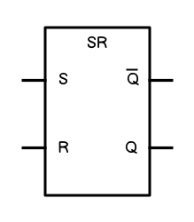
The SR Latch (for “set/reset”) has two inputs: S (for “set”) and R (for “reset”) and one output, Q. Q stands for the bit that is remembered. (There is also not-Q which is the opposite of whatever Q is currently set to.)
The SR Latch goes through the following state changes:
- When S is set to 1, output Q becomes 1 also
- When S goes to 0, Q remains 1
- When R is set to 1, the memory bit is cleared and Q becomes 0.
- Q remains at 0 even if R goes back to 0
This is represented more clearly in the table below:
| S | R | Q | Operation |
|---|---|---|---|
| 1 | 1 | X | Invalid, null |
The most succinct account of a latch:
A latch is a 1-bit memory device that has a state Q of either 1 or 0. The S input sets Q to 1 and the R input resets Q to 0.
The representation of an SR Latch in a digital circuit diagram:

Creating a latch circuit
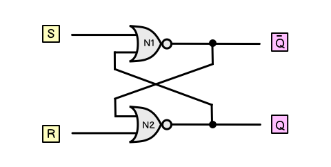
The circuit diagram latch symbol obviously encapsulates more complex functionality that occurs at the sub-circuit level. We will demonstrate how this functionality can be achieved with two NOR gates.
The two gates are in a cross-coupled configuration. This basically means that the wires are crossed back on themselves such that the output of one is also an input of the other at a single stage in the sequence.
The circuit is created as follows:

Interactive version:
Let's talk through the logic at each state change:
- When S is set to 1, output Q becomes 1 also
- N1 is receiving 1 from S and 0 from R by way of N2. This is the inversion of OR so TF equals F. Thus N1 is outputting 0.
- Thus N2 is receiving 0 from N1 as its top input and 0 from R as its bottom input. It is therefore outputting 1 because with NOR, FF equals T. For this reason, Q is 1 because is directly connected to R.
- When S goes to 0, Q remains 1
- N2 is receiving 0 from N1 as the top input and 0 from R as the bottom input hence the overall input is FF which means N2 is outputting T and Q remains 1
- N1 is outputting 0 because it is receiving 0 as its top input and 1 from its bottom input
- When R is set to 1, the memory bit is cleared and Q becomes 0.
- N2 is receiving 1 from R as its bottom input and 1 from the output of N1 as its top input. Therefore it is outputting TT which in NOR evaluates to F hence Q is 0
- N1 is outputting 1 because it is receiving 0 from S as its top input and 0 from its bottom input coming from N2. FF equals T in NOR therefore 1 is outputting 1
- Q remains at 0 even if R goes back to 0
- N2 is receiving 0 as its bottom input from R and 1 as its top input from N1. TF equals F in NOR hence the output of N2 is 0 and Q remains 0
- N1 is outputting 1 because it is receiving 0 as its top input from S and 0 as its bottom input from N2. FF equals T in NOR hence N1 is 1