Hardware Description Language
An HDL is a declarative programming language used to describe the behaviour or structure of digital circuits. They are used to simulate the circuit and check its response.
The hardware designer specifies a chip’s logic by writing an HDL program which is then rigorously tested. At this stage, a hardware simulator takes the HDL program as input and creates a software representation of the chip logic. The designer can instruct the simulator to test the virtual chip on various sets of inputs. This is done to check the chip’s functionality but also to benchmark a variety of other parameters such as speed of computation and energy consumption.
There are many HDLs but the most popular are VHDL (“very high speed integrated-circuit description language”) and Verilog.
Usage in NAND to Tetris
We won’t use an actual HDL language, instead we will use a simplified toy language called HDL that is simple enough that when it is used with a simulator, we can learn the main facets of chip design. Its syntax is very similar to VHDL.
Demonstration of HDL program
Boolean function to enact
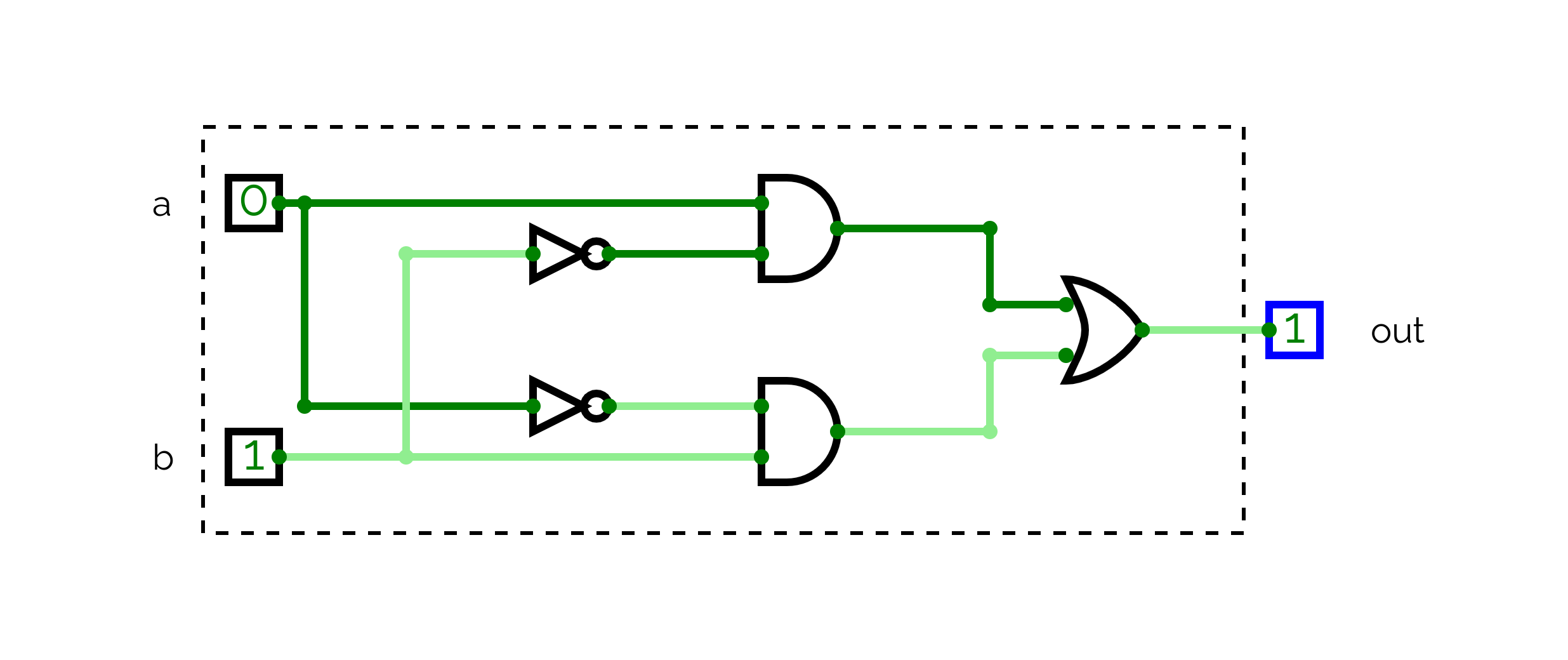
We will create an HDL program for an XOR gate that is implemented through the following arrangement of NOT, AND, and OR gates:

HDL file (Xor.hdl):
Here is our HDL file:
/* Xor gate
   If a!=b out=1 else out=0
*/
CHIP Xor {
  IN a, b;
  OUT out;
  PARTS:
  Not (in=a, out=nota);
  Not (in=b, out=notb);
  And (a=a, b=notb, out=w1);
  And (a=nota, b=b, out=w2);
  Or  (a=w1, b=w2, out=out)
}
Interface (CHIP, IN, OUT)
At the top level of the HDL program, the CHIP name and IN/OUT declaration is the interface of the chip. Here we specify our naming convention for the IN and OUT values which we will refer to in the implementation declaration in PARTS.
Implementation (PARTS)
Everything under the PARTS section is the chip implementation. We can draw on composite gates in the PARTS declaration (e.g. Not, And, Or). The convention is to work from left to right when transcribing from a digital circuit diagram
Pins
In an HDL program we distinguish internal pins along with the standard input and output pins. At the level of the interface, we are concerned only with input and output pins (in the example program these are a, b and out). It is at the level of the implementation that internal pins are encountered. In the example these are the connections between, e.g. the AND and NOT gates such as And (a=a, b-notb, out=w1). This means the AND gate is receiving through its a pin the input a value and through its b pin the value of b inverted by a NOT. out is the value that is computed based on the input pins of a and b.
Test file (Xor.tst)
Along with the HDL file we also create a test file. This runs the chip against the inputs we supply, these will typically be equivalent to the (left-hand) truth-values column in a truth table which is the same as the parameters passed to a Boolean function, for example:
load Xor.hdl
output-list a, b, out;
set a 0, set b 0, eval, output;
set a 0, set b 1, eval, output;
set a 1, set b 0, eval, output;
set a 1, set b =, eval, output;
Output file (Xor.out)
When the test file is run against the HDL file it will generate an output file. This is effectively the result of the unit test. And will take the form of a truth table:
a | b | out
-----------
0 | 0 | 0
0 | 1 | 1
1 | 0 | 1
1 | 1 | 0